| 首页 > 英联产品 > 分立器件 > TVS二极管阵列 > 一般功能保护二极管阵列 |
|
Key Specifications
Product Description The UM5062 ESD protection diode is designed to replace multilayer varistors (MLVs) in portable applications such as cell phones, notebook computers, and PDA’s. It features large cross-sectional area junctions for conducting high transient currents, offers desirable electrical characteristics for board level protection, such as fast response time, lower operating voltage, lower clamping voltage and no device degradation when compared to MLVs.
The UM5062 ESD protection diode protects sensitive semiconductor components from damage or upset due to electrostatic discharge (ESD) and other voltage induced transient events. The UM5062 is available in a QFN3 1.4mm×1.1mm package with working voltages of 5 volt.
It gives designer the flexibility to protect one or two unidirectional line in applications where arrays are not practical. Additionally, it may be “sprinkled” around the board in applications where board space is at a premium. It may be used to meet the ESD immunity requirements of IEC 61000-4-2, Level 4 (±15kV air, ±8kV contact discharge).
Features
- Transient Protection for Data & Power Lines to
IEC 61000-4-2 (ESD) ±15kV (Air), ±8kV (Contact)
- Small Package for Use in Portable Electronics
- Suitable Replacement for MLV’s in ESD Protection Applications
- Protect One or Two I/O Lines
- Low Clamping Voltage
- Stand-off Voltages: 5V
- Low Leakage Current
- Solid-State Silicon-Avalanche Technology
Applications
- Cell Phone Handsets and Accessories
- Microprocessor Based Equipment Personal Digital Assistants (PDA’s)
- Notebooks, Desktops and Servers
- Portable Instrumentation
- Cordless Phones
- Digital Cameras
- Peripherals
- MP3 Players
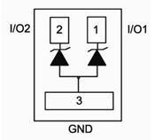
Pin Configurations
(Bottom View)
 Electrical Characteristics
(T=25°C, Device for 5.0V Reverse Stand-off Voltage)
Ordering Information
|
Application Notes
Product Selection Guide
Product Search
Product You Recently Viewed
|